| Home | About Us | Contribute | Bookstore | Advertising | Subscribe for Free NOW! |
| News Archive | Features | Events | Recruitment | Directory |
New MEMS White Paper
Download the latest Logitech white paper and learn more about MEMS processing technology and techniques

| FREE subscription |
| Subscribe for free to receive each issue of Semiconductor Today magazine and weekly news brief. |
News
4 June 2007
UCSB and IQE achieve record fmax of 780GHz for an HBT
The University of California at Santa Barbara’s NanoFabrication Facility has used MBE-grown epitaxial material grown by wafer foundry IQE Inc in Bethlehem, PA, USA on 3” InP wafers to fabricate an Type-I InP/InGaAs/InP double-heterojunction bipolar transistor (DHBT) with a record power-gain cut-off frequency (fmax) of 780GHz for a mesa-structured HBT.
The team reported an fmax of 755GHz at last month’s Indium Phosphide and Related Materials (IPRM) conference in Matsue, Japan (‘Sub-300nm InGaAs/InP Type-I DHBTs with a 150nm collector, 30nm base demonstrating 755GHz fmax and 416GHz ft’, presented by UCSB’s Dr Zach Griffith). However, a bias condition was subsequently found that allowed the HBT to operate at up to 780GHz fmax, Griffith told Semiconductor Today.
“We have collaborated extensively with professor Rodwell’s group for nearly a decade, where many record InP-DHBTs results have been demonstrated over the years,” says Steve Gergar, general manager of IQE’s Pennsylvania operation.
Previous records for fmax were 650 GHz (for an InP DHBT with a 250nm-wide emitter, reported by UCSB at the 64th Device Research Conference in June 2006) and 687GHz (for an InP SHBT, reported by Pohang University of Science and Technology, South Korea and Intelligent Epitaxy Technology of Richardson, TX, USA at the International Electron Devices Meeting in December 2004).
With a simultaneous current-gain cut-off frequency (fT) of 424GHz and a common-emitter breakdown voltage (BVceo) of 5.6V, UCSB’s latest 780GHz fmax device has also demonstrated a record fT x BVceo product ( for a bipolar transistor) of 2.39THzV. (N.B. GaN HEMT devices have higher ft*BVceo products.) The previous record for this figure of merit was 2.30THz*V (fT=384GHz; BVceo=6V) from a Type-II InP DHBT with a 15nm-thick GaAsSb base and an InP collector (Liu et al of Canada's Simon Fraser University, IEEE Transactions on Electron Devices, vol. 53, no. 3, March 2006, p559).
Last December, Milton Feng’s group at the University of Illinois at Urbana-Champaign (UIUC) reported an InGaAs-collector InP-SHBT with a simultaneous 845GHz ft and 263GHz fmax when cooled to -55 degrees Celsius , or 765GHz ft with 227GHz fmax at room temperature. However, a common-emitter breakdown voltage of 1.65V gave an ft*BVceo product of just 1.26THz*V.
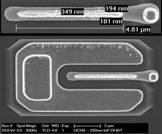
UCSB’s latest 780GHz fmax devices use a graded base-collector junction ( with a 150nm-thick InP collector containing an InGaAs/InAlAs superlattice grade to remove the conduction-band discontinuity between the InP and the 30nm-thick highly doped InGaAs base region) . However, using i-line lithography, the lateral width of the emitter junctions have been scaled from the 500-600nm of the previous ‘generation 2’ InP HBTs to the 250-300nm for ‘generation 3’, while maintaining similar collector-to-emitter area ratios. Because of the subsequent reduction of the base spreading resistance beneath the emitter and increased radial heat flow from the narrower junction, significant increases to fmax and reductions in device thermal resistance are observed.
Most of UCSB’s InP HBT current effort is now focused on the 125nm and 62.5nm emitter-width nodes, Griffith told Semiconductor Today. According to a roadmap presented by UCSB’s professor Mark Rodwell at both IPRM 2007 and this week’s IEEE MTT-S International Microwave Symposium (IMS 2007) in Hawaii, these should yield fmax values of 1.3THz and 1.5THz, respectively, with simultaneous fT values of 730GHz and 1THz. However, work on these 125nm and 62.5nm ‘generation 4’ and ‘generation 5’ devices is still in its infancy, adds Griffith.

Picture: Fabricated HBT before passivation.
*The UCSB/IQE work is supported by program N0001-40-4-10071 of the US Office of Naval Research (ONR), as well as the SWIFT program and the TFAST program N66001-02-C-8080 of the US Defense Advanced Research Projects Agency (DARPA).
See related item:
Record 845GHz transistor reported by UIUC’s Feng
Visit UCSB: http://www.ucsb.edu
Visit IQE: http://www.iqep.com