News: LEDs
6 February 2020
Plessey partners with Axus to process GaN-on-Si monolithic micro-LED displays
At Photonics West 2020 in San Francisco, CA, USA (4-6 February), UK-based Plessey, which develops embedded micro-LED technology for augmented-reality and mixed-reality (AR/MR) display applications, has announced a partnership with Axus Technology of Chandler, AZ, USA (a provider of CMP, wafer thinning and wafer polishing surface-processing solutions) to bring high-performance gallium nitride (GaN)-on-silicon monolithic micro-LED technology to the mass market.
Plessey says that it continues to invest heavily in its manufacturing facility to boost its proprietary micro-LED display capabil ities with the purchase of metal and oxide chemical-mechanical polishing (CMP) and associated tools from Axus to enable the wafer-scale bonding of micro-LED wafers to high-performance CMOS backplanes.
Picture: CMP tool from Axus Technology.
Axus’ CMP and scrubber systems have been deployed to enable critical wafer planarization and preparation for wafer-scale bonding. Wafer-level bonding poses significant technical challenges and, even with the right equipment, requires extensive know-how and refined processes, notes Plessey. Shortly after installation of the systems in 2019, Plessey achieved what is claims was the first functional wafer-level-bonded GaN-on-Si monolithic 1080p 0.7” diagonal 8µm-pixel-pitch micro-LED active-matrix display.
Plessey has further optimized these systems and processes to achieve wafer-to-wafer bonding of a much smaller monochrome native-green 1080p micro-LED display 0.26” diagonal to a 3µm-pixel-pitch backplane display system engineered by Compound Photonics US Corp (CP) of Vancouver, WA, USA (a provider of compact high-resolution microdisplay technologies for AR/MR applications), creating over 2 million individual electrical bonds.

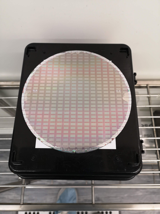
Picture: Electrically and mechanically bonded micro-LED array wafer to 3-micron pixel-pitch backplane.
The formation of the Plessey/Axus partnership has led to the development of critical CMP processes for various materials key to enabling Plessey’s proprietary monolithic GaN-on-Si technology.
Engineers from both firms have collaborated to accomplish these objectives at both Axus’ CMP foundry in Chandler, Arizona and Plessey’s semiconductor fabrication facility in the UK.
Going forward, the partnership will support scaling the technology for high-volume manufacture on the existing Axus equipment set and, in the near future, Axus’ new high-flexibility/throughput Capstone CMP system (launched in late 2019).
“We’ll be working closely with Plessey’s engineers for upgrades to their current tooling and subsequently scaling the technology on Capstone,” says Axus’ president Dan Trojan. “Our ever-expanding investment in our manufacturing facility in the UK is allowing Plessey to innovate rapidly and deliver leading-edge technology for AR and other display applications,” adds Plessey’s chief operating officer Mike Snaith.
Plessey and WaveOptics partner on micro-LED display technology for smart glasses
Plessey develops native red InGaN LEDs on silicon for micro-LED displays
Compound Photonics and Plessey partner on micro-LED displays for AR/MR applications
Plessey’s micro-LED growth technology combines native blue and green epi on single wafer
Jasper Display and Plessey demo first GaN-on-Si monolithic full-HD micro-LED bonded displays
Plessey’s new native green LEDs boosts output for micro-LED displays


