- News
15 November 2017
Improving efficiency of V-band indium gallium nitride transistors and MMICs
HRL Laboratories in the USA has reported V-band (57-64GHz) aluminium gallium nitride (AlGaN) double heterojunction field-effect transistors (DHFETs), claiming “to the best of our knowledge, the best combination of power and PAE reported to date at this frequency [59GHz] for a solid-state device” [M. Micovic et al, IEEE Electron Device Letters, published online 17 October 2017].
The work was supported by Boeing Co. Potential applications in the V-band millimeter-wave radio frequency (RF) electromagnetic radiation band include 5G wireless, collision avoidance radar, and satellite and unmanned aerial vehicle (UAV or ‘drone’) cross links. Increasing efficiency of such devices reduces the thermal management complexity of systems.
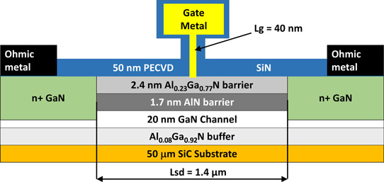
The semiconductor materials (Figure 1) were grown on silicon carbide (SiC) by molecular beam epitaxy (MBE). Silicon carbide is presently the material of choice for III-nitride transistors due to its high thermal conductivity.

Figure 1: Schematic cross section of scaled GaN DHFET.
The Al0.08Ga0.92N buffer also acted as a back-barrier for the device, suppressing hot-electron diffusion and increasing electron confinement in the GaN channel layer through polarization effects. The source and drain regions were etched back and n+-GaN selectively re-grown by MBE for low-resistance access to the channel. The source-drain spacing was 1.4μm.
The T-gate fabrication involved plasma-enhanced chemical vapor deposition (PECVD) silicon nitride passivation, tri-layer resist electron-beam lithography gate definition, dry etch of the silicon nitride for the gate foot, gate metal evaporation, and metal lift-off. The gate metal was protected with a second PECVD silicon nitride passivation layer. The 40nm gate was centered between the source and drain. Previous research by HRL suggests that this gate process flow minimizes current collapse effects from high-frequency signals.
The wafer was thinned and metal applied to the back side, giving an RF and direct current (DC) ground plane. Through-substrate vias were used to connect grounded terminals and passive components to the ground plane. The thinning was down to 50μm, compatible with monolithic microwave integrated circuit (MMIC) technology.
Devices consisted of 4x50μm finger gates, giving a total gate width of 200μm.
The maximum drain current under 10V drain bias was 1.45A/mm. The peak transconductance was 660mS/mm. The threshold and pinch-off voltages for 1mA/mm drain current were -1.04V and -2V, respectively. The negative voltages indicate normally-on depletion-mode behavior.
The 1mA/mm device breakdown was more than 55V when the gate was at -5V. In pulsed operation, current collapse of about 40% was observed. This was greater than in the previous work by HRL on less aggressively scaled devices with 140nm gate length. Also, the barrier layer was thicker – 22nm. The researchers blame surface and passivation traps, arising from the passivation interface being much closer to the channel. The collapse unfortunately reduces the output RF power relative to the available DC input.
The team comments: “Despite relatively high DC to pulsed current collapse of reported devices, we show in this work that aggressive scaling of GaN HEMT results in excellent power performance at V-band.”
With 12V drain bias and 267mA/mm quiescent drain current, testing over the range 50MHz-110GHz gave cut-off and maximum oscillation frequencies of 140GHz and 280GHz, respectively.
A pre-matched 4x50μm-wide transistor circuit was used for V-band power characterization. Measurements at peak power-added efficiency (PAE) gave an output power of more than 23.5dBm (1dBm = 1mW) with associated power gain of more than 5.5dB over 57-64GHz. The maximum power of 25.5dBm was at 59GHz, where the power-added efficiency was 41%. The team comments: “The circuit-level PAE of 41% compares favorably to the highest PAE numbers reported for three-terminal solid-state devices in this frequency range (InP HEMT).”
At the device level, the PAE was 48%. Further measurements and calculations gave associated drain efficiency (DE) of 57%, associated power of 26.17dBm (1.88 W/mm) and associated power gain of 8.1dB. Varying the drain bias between 4V and 16V, the peak PAE was greater than 35% (45% for 6V-16V).
The circuit peak PAE output power was 19dBm (0.4W/mm) at 4V drain, increasing to 27.64dBm (2.9W/mm) at 16V. At the device level, the 16V-bias output power was 28dBm (3.17W/mm) at input power drive 1 dB past the peak PAE point.
The researchers comment: “These results show that a 40nm GaN DHFET is a very attractive device for envelope-tracking V-band power amplifiers, because it maintains excellent PAE over a broad range of drain bias voltages even at fixed matching conditions.” Envelope tracking adjusts the power supply in RF transmission power amplifiers to maintain peak efficiency.
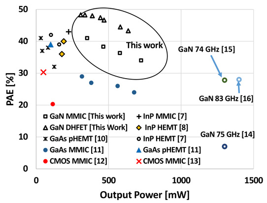
The HRL devices have performance comparable with the best reported high-efficiency transistors and MMICs at V-band (Figure 2).

Figure 2: Comparison of V-band PAE versus output power of best reported high-efficiency transistors and MMICs.
The team concludes: “We anticipate that power performance of the reported GaN DHFETs can be potentially improved by roughly 40% by reducing current collapse using improved surface passivation techniques.”
V-band InGaN transistors MMICs AlGaN DHFETs MBE HRL Laboratories
https://doi.org/10.1109/LED.2017.2763940
The author Mike Cooke is a freelance technology journalist who has worked in the semiconductor and advanced technology sectors since 1997.


