- News
7 November 2013
Normally-off GaN HEMTs with thin high-Al content barrier
China’s Xidian University has produced ‘normally-off’ gallium nitride (GaN) high-electron-mobility transistors (HEMTs) with a thin high-aluminium-content aluminium gallium nitride (AlGaN) barrier layer [Kai Zhang et al, Jpn. J. Appl. Phys., vol52, p111001, 2013].
Normally-off HEMTs are being developed for power switching applications, which need fail-safe operation. Further advantages include lower power consumption and simpler drive circuits.
Unfortunately, simple GaN HEMTs have a negative threshold voltage, giving a normally-on operation. A number of techniques such as fluorine implantation and gate recessing can shift the threshold in a positive direction. However, these methods suffer from thermal stability or process damage problems that impact HEMT performance.
The Xidian approach is similar to gate recessing in that the distance between the gate and channel is reduced. However, gate recessing involves a plasma etch that damages the device structure and leads to higher gate leakage current in operation.
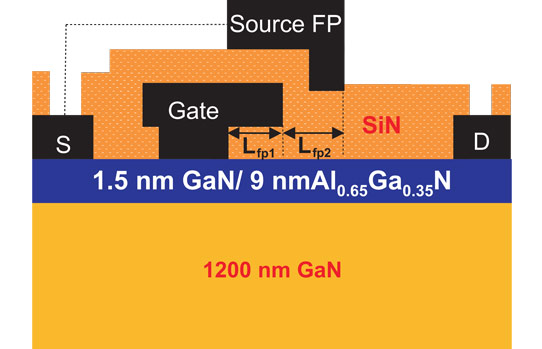
The nitride semiconductor structure (Figure 1) was grown on c-plane sapphire using metal-organic chemical vapor deposition (MOCVD). A 1.5nm GaN cap layer was applied to the top of the AlGaN barrier. The difference in polarization between the GaN cap and AlGaN barrier created a negative polarization charge at the heterointerface that shifted the threshold voltage in a positive direction. The charge was also expected to enhance the Schottky barrier height of the gate, reducing leakage current.

Figure 1: Schematic of fabricated normally-off HEMT with dual field-plates. The growth was initiated on the sapphire substrate using a 200nm AlN nucleation layer.
The ohmic source and drain contacts consisted of annealed titanium/aluminium/nickel/gold. Devices were isolated by plasma etching to a depth of 120nm. Passivation was achieved by plasma-enhanced chemical vapor deposition (PECVD) of silicon nitride (SiN). The passivation reduced the sheet resistance of the two-dimensional electron gas (2DEG) channel by 11% due to a 16% increase in carrier density.
The mobility was slightly reduced by the passivation. It is thought that such passivation reduces the effects of surface states and defects that can deplete the 2DEG. Possible reasons for the reduced mobility include increased electron-electron scattering and/or increased carrier scattering from GaN/AlGaN interface roughness due to the higher carrier density.
The 0.5μm-long gate was formed by creating an opening in the SiN passivation with a plasma etch and depositing nickel/gold/nickel as the gate electrode. Gate and source field-plates (FPs) were included in the design to combat current collapse and to push breakdown to higher voltages. The gate FP overhang was 0.3μm (Lfp1) and the source FP extension was 0.4μm (Lfp2). The gate width was 50μm. The gate-source and gate-drain distances were 0.7μm and 2.6μm, respectively.
The saturation drain current of the device at 5V drain bias (VDS) and 3V gate potential (VGS) was 441mA/mm. The extrinsic maximum transconductance with the same drain bias was 204mS/mm. The threshold was estimated at +0.3V.
The gate leakage at negative gate potentials was 10-7mA/mm at -5V and 10-4mA/mm at -20V. These low values are attributed to the higher estimated Schottky barrier of 0.91eV compared with barriers in the range 0.5-0.7eV for lower Al-fraction AlGaN (15-35%).
The off-state (-2V gate rather than 0V) breakdown voltage for 1mA/mm leakage was 111V. The gate leakage was significantly lower than the drain leakage. The researchers believe this “suggests enhanced breakdown characteristics can be achieved with further optimization in buffer design, such as lowering the defect density, using compensation iron doping, or growing back-barrier layers or double heterojunctions.”
The drain-induced barrier lowering (DIBL) was 3.28mV/V over the drain bias range 1‑20V. The researchers say that this is “greatly superior” to reported values for AlGaN HEMTs with 25nm barrier and 0.6μm gate length. The improved DIBL is attributed to the high quality of the AlGaN and the use of an insulating buffer layer.

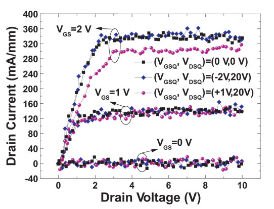
Figure 2: Comparison of pulsed current-voltage characteristics at three quiescent bias points of (VGSQ, VDSQ) = (0V, 0V), (-2V, 20V), and (+1V, 20V), and at VGS = 0, 1, and 2V.
Current collapse effects were investigated under pulsed operation (Figure 2). The off-state test was used to evaluate gate lag. The researchers comment: “The result indicates that the presented Al-rich AlGaN/GaN HEMTs do not suffer from gate lag effects induced by surface-related defects at moderate drain bias, originating from the excellent AlGaN quality, Si3N4 surface passivation as well as the incorporation of a dual-field-plate design.”
The researchers warn that their results were carried out with a relatively low quiescent drain bias of 20V. For power switching applications this should be increased to more than 100V to show the impact of trap charging on dynamic on-resistance.
Current collapse of 12% at 2V gate was seen in the on-state stress testing. “The apparent drain lag effect can be explained as being due to hot-carrier injection into the buffer followed by trapping in deep levels,” the researchers write. The team says that more advanced buffer design is needed to tackle this source of current collapse.
The researchers also looked at thermal stability by performing post-gate annealing in the temperature range 200-450°C in steps of 50°C for 10 minutes each. The tests were carried out in nitrogen atmosphere. During the test the threshold voltage was determined. The threshold shifted only 0.045V in the positive direction. The threshold is thus much more stable compared with fluorine treatments used to give positive threshold HEMTs, indicating higher reliability for the Xidian devices.
Normally-off GaN HEMTs GaN AlGaN MOCVD PECVD
http://jjap.jsap.jp/link?JJAP/52/111001/
The author Mike Cooke is a freelance technology journalist who has worked in the semiconductor and advanced technology sectors since 1997.


