- News
13 April 2011
Dynamic improvement for nitride semiconductor power switching
HRL Laboratories has achieved low dynamic ON-resistance in a nitride semiconductor field-effect transistor with normally-OFF behavior and high breakdown voltage [Rongming Chu et al, IEEE Electron Device Letters, published online 22 March 2011]. The researchers comment: “This is the first time a 1200V normally-OFF GaN-on-Si FET with low dynamic Ron is reported.”
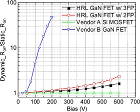
HRL defined its dynamic ON-resistance as being the value attained 5μsecs after switching from OFF to ON. In its best device, HRL achieved a degradation of the ON-resistance of only 1.2x at 350V bias and 1.6x at 600V.
For power switching, the dynamic behavior needs to maintain the good performance achieved in static tests. The ON-resistance can often be degraded in high-voltage power switching from the OFF- to ON-state in nitride transistors due to field-assisted electron trapping in the region between the gate and the drain.
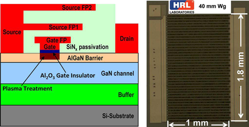
In microwave nitride devices, passivation and field plates have been used to overcome this problem by reducing the effects of charge trap states. This is one reason that HRL used multiple field-plate structures to control the electric fields in its device that was designed (Figure 1) to operate at voltages much higher than those of microwave devices.

Figure 1: Cross-section schematic of device structure (left) and (right) microscopy top-view photograph of GaN-on-Si FET.
The ~4μm AlGaN epi-structures were grown on 3-inch (75mm) (111)-oriented silicon substrates using metal-organic vapor phase deposition (MOCVD). The ohmic source–drain electrodes consisted of annealed titanium/aluminum metal stacks.
The gate formation was begun with a fluorine/chlorine plasma treatment to deplete the channel electrons, providing the normally-OFF characteristic. The researchers see ‘normally-OFF’ operation as being particularly important for safe power switching device technology.
Fluorine is the main factor in providing the depletion and shifting the threshold voltage to positive values. Chlorine has been found to improve transconductance and reduce threshold hysteresis.
The hysteresis factor is caused by charge traps that occur near insulator-semiconductor interfaces, particularly in III-V devices. When there is a large gate bias swing expected in operation, hysteresis must be minimized for stable operation.
HRL’s device has a gate dielectric/insulator of Al2O3, applied using atomic layer deposition (ALD). The 1μm-length gate was completed with a nickel-gold electrode. A silicon nitride passivation layer was grown using plasma-enhance chemical vapor deposition (PECVD), then the field plates were added – one to the gate and two to the source electrode.
The completed devices had a gate width of 40mm and an active area of 1.8mm2. The dies were attached to transistor outline TO-257 metal packages. The source terminal and silicon substrate were bonded to the metal can, while the gate and drain electrode were bonded to the input and output leads.
Process control monitor (PCM) devices were also processed on the wafers. A low threshold hysteresis of 0.1V was measured in these devices, indicating a low interface charge trap density.
Within a gate bias range from –3V up to +3.5V, the maximum drain current at 5V drain bias was 0.18A/mm and the gate leakage was of the order of 10nA/mm. The researchers see low gate leakage as being important for high breakdown voltage, reduced power wastage, and simplified gate drive design.
HRL defined the threshold voltage (Vth) as being the gate potential at which the drain current reaches 1μA/mm at 5V drain bias. In these terms, some 600 PCM devices were tested and found to have 0.64V threshold on average with standard deviation 0.04V. The researchers comment: “The good uniformity of the Vth of the PCM devices suggests the feasibility of constructing normally-OFF FETs with large gate width, as well as the manufacturability of our device fabrication process.”
The static ON-resistance of a packaged device was 0.5Ω or 9mΩ-cm2 at a gate potential of 3V and a drain current of 2A. The catastrophic breakdown at zero gate potential (OFF) was 1200V. The researchers comment: “The low Ron and high breakdown achieved with this device make it a very competitive candidate for high-voltage power-switching applications.”
 HRL compared its device (Figure 2) with varying numbers of field plates, along with commercial silicon superjunction power MOSFET and nitride FET devices. The silicon device showed no dynamic degradation of ON-resistance. The HRL FET with three field plates suffered some degradation of 1.2x at 350V bias and 1.6x at 600V. The researchers comment: “This is, to our knowledge, the best dynamic Ron performance achieved for a normally-OFF GaN FET on Si substrate.”
Figure 2: Ratio between dynamic ON-resistance and static ON-resistance at varied operating biases for different devices.
The HRL team believes that further optimization of the field-plate configuration and epilayer quality could improve these dynamic characteristics towards a degradation-free level.
The author Mike Cooke is a freelance technology journalist who has worked in the semiconductor and advanced technology sectors since 1997.
Join Semiconductor Today's LinkedIn networking and discussion group
