| Home | About Us | Contribute | Bookstore | Advertising | Subscribe for Free NOW! |
| News Archive | Features | Events | Recruitment | Directory |
WAFER PROCESSING
Achieve accurate and repeatable processing results with Logitech's semiconductor equipment.

| FREE subscription |
| Subscribe for free to receive each issue of Semiconductor Today magazine and weekly news brief. |
News
3 June 2008
IMEC and Aixtron claim first
At this week’s International MOVPE conference, taking place in Metz, France, IMEC of Leuven, Belgium and MOCVD equipment maker Aixtron AG of Aachen, Germany demonstrated the growth of high-quality, uniform AlGaN/GaN heterostructures on 200mm silicon (si) wafers.
According to the presentation at Aixtron’s user meeting, IMEC and Aixtron are the first to deposit crack-free AlGaN/GaN structures onto 200mm Si(111) wafers. It was reported that the layers showed good crystalline quality as measured by high-resolution x-ray diffraction, and that excellent morphology and uniformity were obtained. The AlGaN and GaN layers were grown using an Aixtron 300mm CRIUS MOVPE reactor.
For the AlGaN/GaN heterostructures, a standard layer stack that had already been demonstrated on 100 and 150mm Si(111) substrates was used. First, an AlN layer was deposited onto the Si substrate, followed by an AlGaN buffer, which provides compressive stress in the 1 micron thick GaN top layer. The stack was finished with a 20nm thin AlGaN (26% Al) layer and capped with a 2nm GaN layer. Results from in-situ measurements showed that the thickness uniformity of the different layers exhibited a standard deviation below 1% over the full 200mm wafers (5mm EE).
“The demonstration of GaN growth on 200mm Si wafers is an important step towards processing GaN devices on large Si wafers”, said Marianne Germain, program manager of IMEC’s Efficient Power program. “There is a strong demand for GaN-based solid-state switching devices in the field of power conversion. However, bringing GaN devices to a level acceptable for most applications requires a drastic reduction in the cost of this technology. And that is only possible by processing on large-diameter Si wafers. 150mm, and then 200mm are the minimum wafer sizes we need to fully leverage today’s silicon processing capabilities.”
Wafer bow was reported to be in the range of 100μm, but IMEC believes that an optimized buffer can reduce this significantly and enable further processing. Germain added: “We aim to further develop the growth process and to qualify the wafers to be compatible with Si-CMOS process.”
Due to a lack of commercially available GaN substrates, GaN heterostructures are typically grown on sapphire or silicon carbide (SiC), but Si is an attractive alternative because it is less costly, and is available in large quantities and large wafer sizes. Furthermore, the thermal conductivity Si is half of that of SiC. However, until now Si wafers with (111) surface orientation were only available with a diameter up to 150mm. The 200mm Si wafers were custom made by MEMC Electronic Materials Inc using the Czochralski growth (CZ) method. CZ wafers are suited for switching applications with large breakdown voltages. For these devices, performance is independent of the resistivity of the Si substrate.

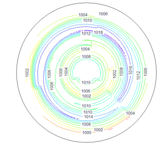
Picture: Thickness uniformity map of a 1μm GaN layer deposited on 200mm Si(111) using an AlN/AlGaN buffer. The average thickness measured in-situ is 1008nm (s = 0.5%) for the full wafer excluding a 5mm edge.
See related items:
Fraunhofer ISE orders Aixtron system for GaAs-on-Si multi-junction solar cell R&D
Aixtron’s orders hit peak after doubling year-on-year
Search: Aixtron MOCVD CRIUS AlGaN/GaN
Visit: www.aixtron.com
Visit: www.imec.be
